Showing posts with label embedded. Show all posts

Friday, 12 February 2016

Embedded Android

                              Having plans to create a device that would change this world ? Are you an embedded programmer skilled in doing some stuffs with micro-controller kits. Time to move on to next level. Next generation arm  based embedded processor kits have arrived. These have already been introduced to run on operating systems like Windows CE, linux, android and more on.

Features of using micro-processors over micro-controllers:

* Connectivity: 

Today, each and every embedded device present before us are connected with each other to form an network. This would be a norm in future which your device must imply with. Connectivity might be either through Wifi, Bluetooth or Ethernet. To add this support to a standalone microcontroller kit would be tiresome. This is the main feature where embedded processors come into play, where the SoC Chip manufacturer handles this for you. These processors are placed on the development board that contains on board Wifi/BT combo chips and come with an Ethernet port. On the Software side, many source operating systems like embedded linux, embedded android are available which provide us with a reliable stack on top of which our applications need to developed. Hence most of our board-bringup and assembling is done by SoC vendors itself. With considerable efforts reduced, our role would be narrowed in developing the application.

* Display :

It would be weird these days if your product comes with a LED/LCD Display to display some text. User Interface [UI] has already been influential because at the end of the day, the user's decision is going to decide the fate of the product. High Resolution Display panels with Resistive/Capacitive Touch Screen would absolutely overthrow its LCD/LED counterparts in this era. These embedded development kits have provisions for connecting several kind of displays ranging from 3" inch to 10" inch. To be noted, they have HDMI ports too which provides rich color resolutions.

* Multimedia :

Have you ever tried to add Audio support for your controller kit?. With these embedded development kits, It is much easier to play audio and video files. Moreover, each kit comes with its own graphical processing unit[GPU] which provides immense gaming performance. To believe it, you need to experience it by playing gaming apps on a development kit running on Android. We prefer Ashphalt !!!!!!

* Storage :

Each embedded processor has its own internal storage in the form of flash[eMMC], whose size from 1GB to 16GB. Hence Data Storage must not be a problem.

* Hardware Interfaces:

Today, Embedded processors come with different interfaces which are not available in conventional microcontroller kits. They include
# USB
# PCI
# SATA

Each of the above interface has its own use case and in turn can provide varied functionalities.

* Camera :

Do you want your device to be bit more realistic manipulating some real time data. Then your device needs to have a camera. These kits have provision for those too.

Myths:

* Power Consumption:

Obviously, microcontrollers outplay these kits in terms of power consumption. But recent technological developments have shed some light onto that area. This might range from advanced suspend/resume operations to low power consuming ARM Cores.Soon this gap would be narrowed down. In the future, you can expect devices that consume almost little amount of energy.

* Complexity of Operating Systems:

Real Time Operating systems tend to be more complex from a developer point of view. But in reality, you have got more advantages than disadvantages. Nowadays, several Developer communities are available which openly offer support to any kind of problems faced while developing a device.

* Cost :

Embedded Development kits actually tend to be cost-effective because they provide end-to-end solution for making device. It is really good to see low cost development kits to hit the market. Front runners among them are Raspberry Pi and Snapdragon Board.

The continuation of these posts mainly target embedded developers who are aspiring to bring out some new innovation to this world like us. To begin with, we recommend you with the following kits.


  •  Freescale imx6 based processors.
  •  Wandboard Solo,Dual or Quad.
  •  Nitrogen 6x Kits
  •  UDOO imx6 kits.
  •  Ankaa Development Kit 
  •  Raspberry Pi
  •  Qualcomm Snapdragon


Regarding the Operating system, we prefer "Embedded Android". To know why, wait for the next post..

Saturday, 12 July 2014

Interfacing RTC DS1307 with Atmel AVR Microcontroller

Interfacing RTC DS1307 with Atmel AVR Microcontroller

         In this tutorial, the steps involved in interfacing the real time clock chip DS1307 with Atmel AVR microcontroller has been explained. Before getting into detail,

What is this RTC??

A real-time clock(RTC) basically as the name suggests are clock modules that keeps track of the current time. These RTCs are present in almost any embedded device which needs to keep accurate time. The main advantage of RTC is that they have a battery backup which keeps the clock running even in case of power failure.There are many RTC chips available in the market, but DS1307 is the one most commonly used.

Features of DS1307: 
DS1307 is serial real time clock which is I2C compatible. So before continuing this blog have a quick look at our previous post about I2C Communication to get a clear picture visit our page
This provides seconds, minutes, hour, day, date, month and year information. The end of the month is automatically adjusted which are fewer than 31 days including leap year.
The clock inside the chip supports both 24 hr and 12 hr format with AM/PM indicator.
The chip has an in-built power sense circuit which senses the power failure and switches to battery backup power.
Steps involved in Interfacing RTC with AVR controller:
The RTC DS1307 has a set of internal time keeping registers which is used to set and read time from them. They also have 58 bytes of non-volatile RAM to store information such as an alarm, event reminder something like that.


Note: As said on the DS1307 datasheet, because the initial power-on state of this bit is not defined, it is important to clear the Clock Halt (CH=0) bit in the seconds register(00H).

    2) Once the registers been properly set, we can read the time directly. One important thing is these registers don’t store the values as binary. Instead it stores all its values in Binary Coded Decimal (BCD) format. So care should be taken while writing the time into these registers.

     3) As I have already explained the protocol used in this interface is I2C.

·        RTC DS1307 à acts as I2C Slave
·        AVR controller à acts as I2C Master

     4) Writing the time into the Slave’s corresponding registers:


  • ·        In any communication normally there has to be a sender and recipient, and both should have an initial pairing only then the communication will be effective.
  • ·        This initial pairing has to be done by the master by specifying the slave address which it wants to communicate. In our case the slave address for DS1307 is a 7 bit address 1101000.

  • ·        Once the slave address is given, we have to specify whether it is a read/write operation(in our case, Write=0).
  • ·        After getting the ACK, specify the register address from where the write operation has to start.
  • ·        For every ACK, send a data to the slave. It automatically increments the address pointer so there is no need for specifying the register address each time.
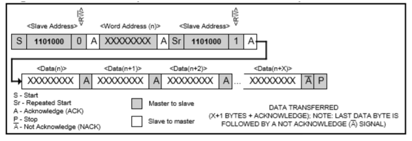
      5) Reading the time from the Slave’s corresponding registers:

  • ·        For read operation, when we don’t specify the address pointer from which it has to be read, the data will start reading from the last pointed address which might not be valid.
  • ·        Hence it is advisable to specify the address pointer first before the start of any read operation.

  • ·        This could be done by writing the register address(in write mode) in order to point the address pointer to the location we need and then switching it to read mode(Read=1) by performing the repeated start operation.
  • ·        The process is same as the write operation. One thing to be noted is that the last data has to be negative acknowledged NACK in read mode.
  • ·        That’s all, the interfacing part of RTC is completed now. You can view this real time clock running in your display.
For any doubts either conceptually or in the coding side, you can contact us at embeddedunderoneroof@gmail.com

Author
Karthik

Embedded Project Engineer

Wednesday, 2 July 2014

I2C COMMUNICATION (Explanation With Diagrams)

I2C is primarily used for communication between two Integrated Chips. I2C protocol was designed by Philips. This post will help you to easily interface two IC’s using I2C protocol.
I2C is a two wire communication system where master controls the slave. The two wires are SDA and SCL. These two wires are pulled up using resistors, which forms wired AND connection between Master and Slaves.
IMPORTANT TERMS: 
SDA- Serial Data Line.
SCL- Serial Clock Line.
Master- Master is a device which take care of data transfer between IC’s by providing proper clock signal
Slave- Slave is a device where the data can be written and read.
Clock- Clock is a Periodic signal generated by the Master, the state of the clock plays a major role in STARTING, TERMINATING and SAMPLING the data.
Data- Data is also a signal where the data, either 1 or 0 is represented.
COMMUNICATION: 
What is I2C Connection?
i2c-diagram
In-order to start a communication between two IC’s they should be connected as per the I2C Protocol.
What Determines the number of Slaves in a line? 
ADDRESS LINES, based on the number of address lines number of devices can be calculated, using the formula 2 ^address lines. In this post I will explain about 7 bit addressing.
How to Initiate a Communication? 
Communication is initiated by first addressing the desired IC. The desired IC is addressed by using the device address, normally the device address will be mentioned by the manufacturer, for example Device Address of a RTC (DS1307) will be 1101000. Once identifying the device address the following procedure has to be followed.
STEPS: 
  1. Transmit the Start Bit
  2. Transmit the Device address(specifying the read or write mode).
  3. Receive the acknowledgement.
  4. Transmit the Register Address(optional).
  5. Receive the acknowledgement.
  6. Transmit the Data as per your wish.(for each byte receive an acknowledgement)
  7. Transmit the Stop Bit.
1) Transmitting the Start Bits and Stop Bits: 
Start Bit: A State know as Start Bit is generated when the data line is pulled from HIGH to LOW when the Clock is HIGH
Stop Bit: A State know as Stop Bit is generated when the data line is pulled from LOW to HIGH when the Clock is HIGH
i2c-tutorial-star-stop                                        .
note: From the above Diagram it can be inferred that it is not advisable to change the state of SDA when the clock is HIGH as it either starts or ends the connection. 
2)Transmitting the Device Address: 
Once the Start Bit is transmitted it must be followed by the device address along with the read/write bit. well, here we shall take RTC as an example. RTC mentioned above has 7bit address this seven bit address has to be transmitted serially bit by bit through SDA line.
IMPORTANT WHILE TRANSMITTING THE DATA:( The data can be device address, register address or the byte which has to be stored in the register)
  • The MSB of the byte must be sent first.
  • The state of SDA line must not be changed when the Clock signal is HIGH.
  • The State of SDA should be changed only if the state of the Clock is LOW
Once the 7 bit of address is transmitted then READ/WRITE bit has to be send. This bit determines whether the data is read from the slave or written from the slave.
  • READ - 
  • WRITE - 0 
ACKNOWLEDGEMENT: 
Once the device address is transmitted the slave has to acknowledge the user by sending the acknowledgement bit. Transmitting the device address will take 8 clock pulse , therefore in the 9th clock pulse acknowledgement must be received by the master. The Slave device will pull the SDA line to LOW to Acknowledge the data transmitted.
  • POSITIVE ACKNOWLEDGEMENT: Bit 0 is sent.
  • NEGATIVE ACKNOWLEDGEMENT: Bit 1 is sent.
3)Transmitting the Register Address: 
It is similar to the transmission of device address but it doesn`t include the READ/WRITE bit. Here the eight bit address has to be transmitted serially bit by bit through SDA line.
After transmitting it acknowledgement is received by the master.
4) Transmitting the Data as per your wish: 
The data is sent similar to the address and an acknowledgement is received after 8 bits. We can transmit N number of data and  finally conclude it with a stop bit . The register address need not be mentioned every time, the slave device can increment the address automatically. But if you need to write in a specific address or if the slave device does not increment the address you have to mention the register address.
Thus the  data is written to the slave device. then Stop Bit has to be sent as mentioned above.
READING THE DATA FROM THE IC 
  1. Transmit the Start Bit
  2. Transmit the Device address(specifying the write mode).
  3. Receive the acknowledgement.
  4. Transmit the Register Address.
  5. Receive the acknowledgement.
  6. Transmit the Start Bit again. (Repeated Start)
  7. Transmit the Device address.(specifying the read mode).
  8. Read the Data as per your wish.(Master should send acknowledgement for each byte it read)
  9. Perform the steps 1 to 6 to read the desired registers.
  10. once the reading is done master should send negative acknowledgement to the IC.
  11. Transmit the Stop Bit.
NOTE: Transmitting the start bits, stop bits, device address, register address  explained above can be used for reading the data from the IC. 
Reading the data from the IC: 
The data is read from the IC bit by bit and an acknowledgement is sent by the master to the IC after 8 bits. We can read N number of data and  finally conclude it by sending a NEGATIVE ACKNOWLEDGEMENT. The register address need not be mentioned every time, the slave device can increment the address automatically. But if you need to read from a specific address or if the slave device does not increment the address you have to mention the register address.  Thus the  data is read from the slave device. Then Stop Bit has to be sent as mentioned above to stop the communication.


The above diagram shows the start bit, transmission of device address(0xA0,WRITE mode), transmission of register address(0×0000), then transmitting the data(0×41) and finally the stop bits of EEPROM 24C256
CLOCK STRETCHING: 
While reading data from the slave, the slave might take some extra time than the one prescribed in the data sheet. In such a case the slave has the ability to hold the clock low until It puts the data in the SDA line. this process is known as CLOCK STRETCHING.
AUTHOR
Hari Prasath
Project Engineer